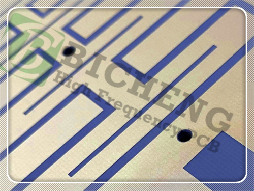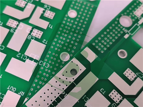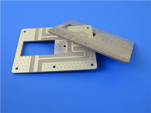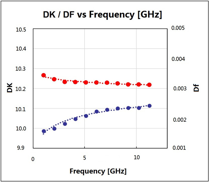
2-Layer RF-10 PCB 0.3mm Thin Immersion Gold Finish for High-Frequency RF Applications1.Introduction RF-10 copper clad laminates are composites of ceramic-filled PTFE and woven fiberglass, engineered to deliver superior performance in high-frequency RF applications. These laminates excel in size reduction for RF circuits while maintaining low dielectric loss and excellent dimensional stability. The smooth, low-profile copper bonding ensures minimal insertion losses, especially critical at higher frequencies where skin effect losses dominate. RF-10 is a cost-effective substrate with industry-leading delivery times, making it a preferred choice for demanding RF and microwave designs. 2.Key Features Dielectric Constant: 10.2 ± 0.3 at 10GHz, enabling compact circuit designs. 3.Benefits Size Reduction: High DK allows for smaller RF circuit designs.
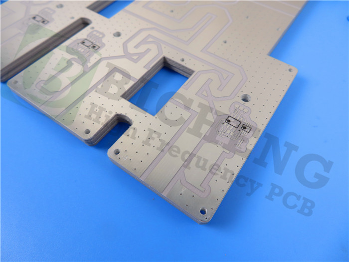
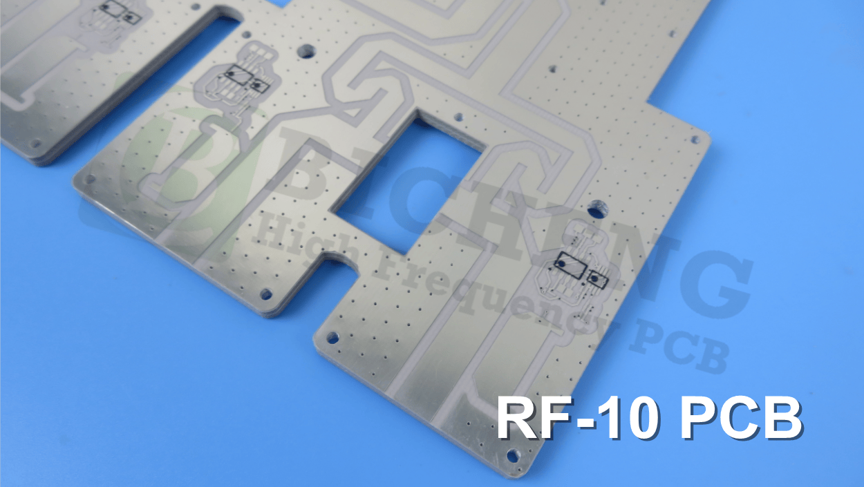
4.PCB Construction Details
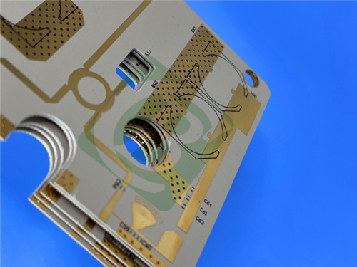
5.PCB Stackup (2-Layer Rigid Structure) Copper layer 1 - 35μm (1oz) 6.PCB Statistics: Components: 7 7.Typical Applications Microstrip Patch Antennas 8.Quality Assurance IPC-Class 2 compliant |
Get a Quick Quote
Fill in the form below and our engineers will reply within 24 hours with technical specifications and pricing for 2-Layer RF-10 PCB 0.3mm Thin Immersion Gold Finish.